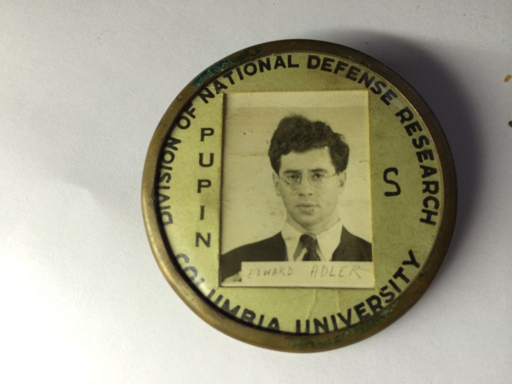
Edward Adler (1916-1998) was an American electrochemical engineer. During the Manhattan Project, Adler worked in a laboratory at Columbia University under Professor Harold Urey and Dr. John Dunning. In collaboration with Edward Norris, Adler pioneered an electroplated nickel mesh barrier to be used in the separation of fissionable uranium-235 from its more stable isotope, uranium-238. While their design was passed over for the nickel-powder barrier designed by Clarence Johnson at the Kellex Corporation, Adler certainly helped lay the groundwork for the barrier that was used.
He was so energetic and excited about the project that he often literally lived in his Columbia laboratory.
Early life
As a boy, Adler worked in family-run candy shops where he frequently read pulp science-fiction magazines and cultivated his abiding interest in science. In 1935 he graduated near the top of his class at the College of the City of New York, where he went on to teach physical chemistry. Adler was a member of both Phi Beta Kappa and Sigma Xi throughout his academic career. He also won the Ward Medal for the student showing the most proficiency in chemistry and the Award of the American Institute of Chemists for his scholastic achievements. After working for a number of years, Adler attended graduate school at Columbia University, where he received his Ph.D. in 1941. He also won the Young Author’s Prize from the Electro-Chemical Society for his doctoral thesis.
Later Years
After the war, Adler turned his knowledge of electroplating, printing, and photolithography to numerous commercial endeavors, including the production of foil nameplates. In 1954 Adler founded the Copper Foil Corporation which produced high performance electrodeposited copper foil, one of the essential components in printed circuit board manufacturing. Adler accumulated numerous patents throughout his professional career, the most prominent being his technique for producing adhesive copper foil. Adler’s inventions revolutionized electronic equipment, contributing to the designs of the computers and cell phones we use today.
The above information was provided by Edward’s family.


